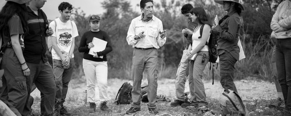

Big things are happening on a minute – or nano – scale. The Stanford community and the public can learn about this cutting-edge research during the nano@stanford open house on Oct. 9. Visitors can take tours featuring high-resolution microscope demonstrations and handle (with tweezers) silicon wafers used in semiconductors. Stanford’s shared resource platforms, C-ShaRP, will also host a series of brief research talks.
Nanotechnology, the manipulation and visualization of matter at the atomic and molecular level, is already part of everyday life, from electronics to medicine. In this Q&A, Debbie Senesky, the site director and principal investigator of nano@stanford, discusses how nanotechnology is shaping our world – and its potential for future breakthroughs, even in space.
A nanometer is one billionth, or 10-9, of a meter. How do you help people conceptualize something so small?
The human eye, without high-resolution instruments, cannot see things at the nanoscale. The diameter of the human hair is around 75 micrometers. So, we need to go three orders of magnitude smaller to reach the nanoscale. A single gold atom is about a third of a nanometer in diameter. Also, a strand of human DNA is around 2.5 nanometers in diameter. We’re talking about things near the atomic level.
Do things operate differently at that scale? Are physical forces different?
Yeah, at such a minute scale, we move away from bulk effects. The behavior of materials changes as the scale decreases, and we start to see quantum, or subatomic, effects. At a smaller scale, surface area dominates and can alter fluidic behavior and chemical absorption. Also, electrical, thermal, and optical properties can become enhanced due to quantum effects. For example, the conductivity of gold can change if the metal takes the form of a nanowire or dot, as opposed to a larger, millimeter-scale wire.
These are the reasons why we like to engineer at the nanoscale – to exploit these new and often better properties.
How might someone encounter nanotechnology in everyday life?
Nanotechnology is everywhere. It’s a part of our cellphones, our laptops, our cars. Imagine opening up your cellphone to see the microelectronics or “chips” inside. If you zoom in on a chip, you might see the layers of metal or patterned features on that chip that are at the nanometer scale. Your cellphone exploits nanotechnology and the ability to deposit very thin metal films and pattern nanoscale features on semiconductor substrates to make devices like transistors.
We want to bring awareness because communities may not think they have access to nano@stanford, but they actually do.”
Debbie Senesky
In what areas do you think nanotechnology will have the most impact in the coming years?
I think that nanotechnology will have a great impact in the field of semiconductors that are the heart of all of the electronics we use. When we start to make chips with devices that are very, very small, overheating can degrade the chips’ performance and lifetime. Researchers are trying to create new types of semiconductor devices with new materials such as diamond to overcome some of those barriers. Nanotechnology can help us visualize and make these new chips. In addition, I think we’ll have new discoveries in our understanding of biology and medicine, and even the evolution of our planet by examining rocks with nanotechnology. One day, we might even use nanomaterials to make a space elevator. The roadblock is that our materials just aren’t strong enough at such a large scale.
What would a space elevator do?
Right now, we have the International Space Station that’s orbiting Earth, but imagine if you had a space platform that was connected to Earth via a strong tether. Instead of sending objects on a rocket, we could send them up to space on, literally, an elevator. People hypothesize we would use materials like carbon nanotubes or graphene composites that are stronger than steel to create something like a space elevator. It’s a very sci-fi concept.
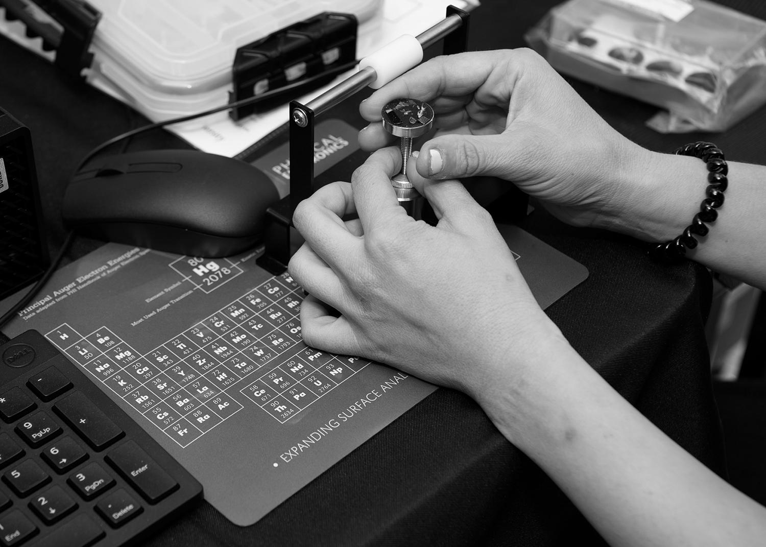
At last fall’s open house, a researcher adjusts the height of a scanning electron microscope sample stub to ensure the proper distance between the sample and the electron beam. This sample stub contains several samples, including a Blue Morpho butterfly wing (which has nano structures used to create color), a section of an etched silicon wafer, and various biological samples like parts of a flower and insect. | Courtesy nano@stanford
Can you give me an overview of the work being done in nanotechnology at Stanford and what excites you most about it?
Our nanotechnology research at Stanford is a very interdisciplinary effort. Topics range from materials science, electrical engineering, physics, biology, medicine, and even policy and ethics. At the upcoming open house, our keynote speaker will describe some very cool interdisciplinary work that came out of Stanford. They’ve developed a method to make skin temporarily transparent, paving the way for non-invasive diagnostics. We may use this new ability to visualize the state of organs, vessels, or even tumors that may be growing in the body and develop new medical procedures.
The open house welcomes the entire community. Why is it important for everyone to know about this kind of research?
What’s unique about nano@stanford is that it’s an open, shared facility. It’s open not only to the Stanford community. We also have many external users who regularly use our facility. For example, we have more than 100 startup companies in our user base. Since buying clean room equipment can be extremely costly, startups can pay monthly fees to use our facilities for prototyping. Also, we conduct a lot of education and outreach. We have a paid internship program where we have community college students working within our labs along with our staff members to support research. In concert with their education skills, that can translate to jobs in the semiconductor workforce or medical fields. So, we want to bring awareness because communities may not think they have access to nano@stanford, but they actually do.
“Stanford University, officially Leland Stanford Junior University, is a private research university in Stanford, California. The campus occupies 8,180 acres, among the largest in the United States, and enrols over 17,000 students.”
Please visit the firm link to site