As computer chips continue to get smaller and more complex, the ultrathin metallic wires that carry electrical signals within these chips have become a weak link. Standard metal wires get worse at conducting electricity as they get thinner, ultimately limiting the size, efficiency, and performance of nanoscale electronics.
“We are breaking a fundamental bottleneck of traditional materials like copper,” said Asir Intisar Khan, who received his doctorate from Stanford and is now a visiting postdoctoral scholar and first author on the paper. “Our niobium phosphide conductors show that it’s possible to send faster, more efficient signals through ultrathin wires. This could improve the energy efficiency of future chips, and even small gains add up when many chips are used, such as in the massive data centers that store and process information today.”
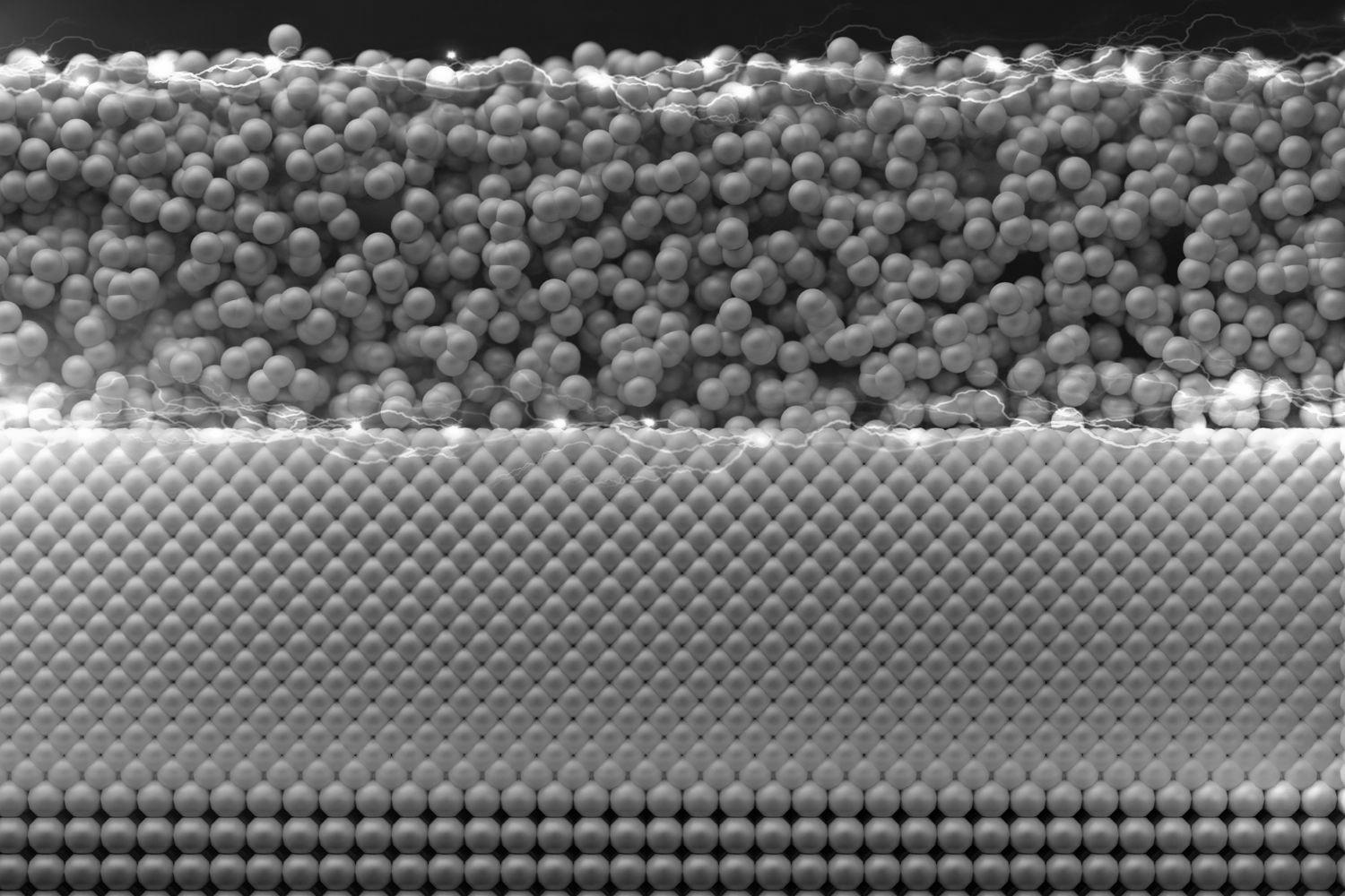
Niobium phosphide is what researchers call a topological semimetal, which means that the whole material can conduct electricity, but its outer surfaces are more conductive than the middle. As a film of niobium phosphide gets thinner, the middle region shrinks but its surfaces stay the same, allowing the surfaces to contribute a greater share to the flow of electricity and the material as a whole to become a better conductor. Traditional metals like copper, on the other hand, become worse at conducting electricity once they are thinner than about 50 nanometers.
The researchers found that niobium phosphide became a better conductor than copper at film thicknesses below 5 nanometers, even when operating at room temperature. At this size, copper wires struggle to keep up with rapid-fire electrical signals and lose a lot more energy to heat.
“Really high-density electronics need very thin metal connections, and if those metals are not conducting well, they are losing a lot of power and energy,” said Eric Pop, the Pease-Ye Professor in the School of Engineering, a professor of electrical engineering, and senior author on the paper. “Better materials could help us spend less energy in small wires and more energy actually doing computation.”
“,”additional”:{“file_info”:{“file_name”:”NbpConductors_Schematic_1500_1.jpg”,”size_readable”:”255.5 KB”,”size_bytes”:261584,”width”:1500,”height”:1000,”modified_readable”:”Jan 6, 2025 2:19 PM”,”modified_unix”:1736201957},”varieties”:[{“id”:”163609:v1″,”type”:”image_variety”,”type_name”:”Image Variety”,”version”:””,”name”:”100w”,”short_name”:”100w”,”status”:{“id”:16,”code”:”live”,”name”:”Live”},”created”:{“date”:”1969-12-31T16:00:00-08:00″,”user_id”:null},”updated”:{“date”:”1969-12-31T16:00:00-08:00″,”user_id”:null},”published”:{“date”:null,”user_id”:null},”status_changed”:{“date”:”1969-12-31T16:00:00-08:00″,”user_id”:null},”urls”:[“https://news.stanford.edu/__data/assets/image/0025/163609/varieties/100w.jpg”],”url”:”https://news.stanford.edu/__data/assets/image/0025/163609/varieties/100w.jpg”,”attributes”:{“variety_type”:”resize”,”filename”:”100w.jpg”,”name”:”100w”,”title”:”Schematic”,”caption”:”Credit: Il-Kwon Oh/Asir Khan”,”variety_size”:4676,”variety_height”:100,”variety_width”:100,”alt”:”A few atoms thick film of non-crystalline NbP conducts better through the surface to make the material, as a whole, a better conductor.”,”dimension_min”:0,”dimension”:100,”height”:0,”width”:0,”constrain”:”centre_weighted_square”},”metadata”:null,”contents”:””,”additional”:{}},{“id”:”163609:v2″,”type”:”image_variety”,”type_name”:”Image Variety”,”version”:””,”name”:”150w”,”short_name”:”150w”,”status”:{“id”:16,”code”:”live”,”name”:”Live”},”created”:{“date”:”1969-12-31T16:00:00-08:00″,”user_id”:null},”updated”:{“date”:”1969-12-31T16:00:00-08:00″,”user_id”:null},”published”:{“date”:null,”user_id”:null},”status_changed”:{“date”:”1969-12-31T16:00:00-08:00″,”user_id”:null},”urls”:[“https://news.stanford.edu/__data/assets/image/0025/163609/varieties/150w.jpg”],”url”:”https://news.stanford.edu/__data/assets/image/0025/163609/varieties/150w.jpg”,”attributes”:{“variety_type”:”resize”,”filename”:”150w.jpg”,”name”:”150w”,”title”:”Schematic”,”caption”:”Credit: Il-Kwon Oh/Asir Khan”,”variety_size”:8737,”variety_height”:150,”variety_width”:150,”alt”:”A few atoms thick film of non-crystalline NbP conducts better through the surface to make the material, as a whole, a better conductor.”,”dimension_min”:0,”dimension”:150,”height”:0,”width”:0,”constrain”:”centre_weighted_square”},”metadata”:null,”contents”:””,”additional”:{}},{“id”:”163609:v3″,”type”:”image_variety”,”type_name”:”Image Variety”,”version”:””,”name”:”200w”,”short_name”:”200w”,”status”:{“id”:16,”code”:”live”,”name”:”Live”},”created”:{“date”:”1969-12-31T16:00:00-08:00″,”user_id”:null},”updated”:{“date”:”1969-12-31T16:00:00-08:00″,”user_id”:null},”published”:{“date”:null,”user_id”:null},”status_changed”:{“date”:”1969-12-31T16:00:00-08:00″,”user_id”:null},”urls”:[“https://news.stanford.edu/__data/assets/image/0025/163609/varieties/200w.jpg”],”url”:”https://news.stanford.edu/__data/assets/image/0025/163609/varieties/200w.jpg”,”attributes”:{“variety_type”:”resize”,”filename”:”200w.jpg”,”name”:”200w”,”title”:”Schematic”,”caption”:”Credit: Il-Kwon Oh/Asir Khan”,”variety_size”:10400,”variety_height”:133,”variety_width”:200,”alt”:”A few atoms thick film of non-crystalline NbP conducts better through the surface to make the material, as a whole, a better conductor.”,”dimension_min”:0,”dimension”:0,”height”:200,”width”:200,”constrain”:”width”},”metadata”:null,”contents”:””,”additional”:{}},{“id”:”163609:v4″,”type”:”image_variety”,”type_name”:”Image Variety”,”version”:””,”name”:”300w”,”short_name”:”300w”,”status”:{“id”:16,”code”:”live”,”name”:”Live”},”created”:{“date”:”1969-12-31T16:00:00-08:00″,”user_id”:null},”updated”:{“date”:”1969-12-31T16:00:00-08:00″,”user_id”:null},”published”:{“date”:null,”user_id”:null},”status_changed”:{“date”:”1969-12-31T16:00:00-08:00″,”user_id”:null},”urls”:[“https://news.stanford.edu/__data/assets/image/0025/163609/varieties/300w.jpg”],”url”:”https://news.stanford.edu/__data/assets/image/0025/163609/varieties/300w.jpg”,”attributes”:{“variety_type”:”resize”,”filename”:”300w.jpg”,”name”:”300w”,”title”:”Schematic”,”caption”:”Credit: Il-Kwon Oh/Asir Khan”,”variety_size”:10400,”variety_height”:133,”variety_width”:200,”alt”:”A few atoms thick film of non-crystalline NbP conducts better through the surface to make the material, as a whole, a better conductor.”,”dimension_min”:0,”dimension”:0,”height”:300,”width”:200,”constrain”:”width”},”metadata”:null,”contents”:””,”additional”:{}},{“id”:”163609:v5″,”type”:”image_variety”,”type_name”:”Image Variety”,”version”:””,”name”:”345w”,”short_name”:”345w”,”status”:{“id”:16,”code”:”live”,”name”:”Live”},”created”:{“date”:”1969-12-31T16:00:00-08:00″,”user_id”:null},”updated”:{“date”:”1969-12-31T16:00:00-08:00″,”user_id”:null},”published”:{“date”:null,”user_id”:null},”status_changed”:{“date”:”1969-12-31T16:00:00-08:00″,”user_id”:null},”urls”:[“https://news.stanford.edu/__data/assets/image/0025/163609/varieties/345w.jpg”],”url”:”https://news.stanford.edu/__data/assets/image/0025/163609/varieties/345w.jpg”,”attributes”:{“variety_type”:”resize”,”filename”:”345w.jpg”,”name”:”345w”,”title”:”Schematic”,”caption”:”Credit: Il-Kwon Oh/Asir Khan”,”variety_size”:26202,”variety_height”:230,”variety_width”:345,”alt”:”A few atoms thick film of non-crystalline NbP conducts better through the surface to make the material, as a whole, a better conductor.”,”dimension_min”:0,”dimension”:0,”height”:555,”width”:345,”constrain”:”width”},”metadata”:null,”contents”:””,”additional”:{}},{“id”:”163609:v6″,”type”:”image_variety”,”type_name”:”Image Variety”,”version”:””,”name”:”375w”,”short_name”:”375w”,”status”:{“id”:16,”code”:”live”,”name”:”Live”},”created”:{“date”:”1969-12-31T16:00:00-08:00″,”user_id”:null},”updated”:{“date”:”1969-12-31T16:00:00-08:00″,”user_id”:null},”published”:{“date”:null,”user_id”:null},”status_changed”:{“date”:”1969-12-31T16:00:00-08:00″,”user_id”:null},”urls”:[“https://news.stanford.edu/__data/assets/image/0025/163609/varieties/375w.jpg”],”url”:”https://news.stanford.edu/__data/assets/image/0025/163609/varieties/375w.jpg”,”attributes”:{“variety_type”:”resize”,”filename”:”375w.jpg”,”name”:”375w”,”title”:”Schematic”,”caption”:”Credit: Il-Kwon Oh/Asir Khan”,”variety_size”:30405,”variety_height”:250,”variety_width”:375,”alt”:”A few atoms thick film of non-crystalline NbP conducts better through the surface to make the material, as a whole, a better conductor.”,”dimension_min”:0,”dimension”:0,”height”:200,”width”:375,”constrain”:”width”},”metadata”:null,”contents”:””,”additional”:{}},{“id”:”163609:v7″,”type”:”image_variety”,”type_name”:”Image Variety”,”version”:””,”name”:”400w”,”short_name”:”400w”,”status”:{“id”:16,”code”:”live”,”name”:”Live”},”created”:{“date”:”1969-12-31T16:00:00-08:00″,”user_id”:null},”updated”:{“date”:”1969-12-31T16:00:00-08:00″,”user_id”:null},”published”:{“date”:null,”user_id”:null},”status_changed”:{“date”:”1969-12-31T16:00:00-08:00″,”user_id”:null},”urls”:[“https://news.stanford.edu/__data/assets/image/0025/163609/varieties/400w.jpg”],”url”:”https://news.stanford.edu/__data/assets/image/0025/163609/varieties/400w.jpg”,”attributes”:{“variety_type”:”resize”,”filename”:”400w.jpg”,”name”:”400w”,”title”:”Schematic”,”caption”:”Credit: Il-Kwon Oh/Asir Khan”,”variety_size”:33504,”variety_height”:267,”variety_width”:400,”alt”:”A few atoms thick film of non-crystalline NbP conducts better through the surface to make the material, as a whole, a better conductor.”,”dimension_min”:0,”dimension”:0,”height”:100,”width”:400,”constrain”:”width”},”metadata”:null,”contents”:””,”additional”:{}},{“id”:”163609:v8″,”type”:”image_variety”,”type_name”:”Image Variety”,”version”:””,”name”:”555w”,”short_name”:”555w”,”status”:{“id”:16,”code”:”live”,”name”:”Live”},”created”:{“date”:”1969-12-31T16:00:00-08:00″,”user_id”:null},”updated”:{“date”:”1969-12-31T16:00:00-08:00″,”user_id”:null},”published”:{“date”:null,”user_id”:null},”status_changed”:{“date”:”1969-12-31T16:00:00-08:00″,”user_id”:null},”urls”:[“https://news.stanford.edu/__data/assets/image/0025/163609/varieties/555w.jpg”],”url”:”https://news.stanford.edu/__data/assets/image/0025/163609/varieties/555w.jpg”,”attributes”:{“variety_type”:”resize”,”filename”:”555w.jpg”,”name”:”555w”,”title”:”Schematic”,”caption”:”Credit: Il-Kwon Oh/Asir Khan”,”variety_size”:57888,”variety_height”:370,”variety_width”:555,”alt”:”A few atoms thick film of non-crystalline NbP conducts better through the surface to make the material, as a whole, a better conductor.”,”dimension_min”:0,”dimension”:0,”height”:0,”width”:555,”constrain”:”width”},”metadata”:null,”contents”:””,”additional”:{}},{“id”:”163609:v9″,”type”:”image_variety”,”type_name”:”Image Variety”,”version”:””,”name”:”600w”,”short_name”:”600w”,”status”:{“id”:16,”code”:”live”,”name”:”Live”},”created”:{“date”:”1969-12-31T16:00:00-08:00″,”user_id”:null},”updated”:{“date”:”1969-12-31T16:00:00-08:00″,”user_id”:null},”published”:{“date”:null,”user_id”:null},”status_changed”:{“date”:”1969-12-31T16:00:00-08:00″,”user_id”:null},”urls”:[“https://news.stanford.edu/__data/assets/image/0025/163609/varieties/600w.jpg”],”url”:”https://news.stanford.edu/__data/assets/image/0025/163609/varieties/600w.jpg”,”attributes”:{“variety_type”:”resize”,”filename”:”600w.jpg”,”name”:”600w”,”title”:”Schematic”,”caption”:”Credit: Il-Kwon Oh/Asir Khan”,”variety_size”:63439,”variety_height”:400,”variety_width”:600,”alt”:”A few atoms thick film of non-crystalline NbP conducts better through the surface to make the material, as a whole, a better conductor.”,”dimension_min”:0,”dimension”:0,”height”:0,”width”:600,”constrain”:”width”},”metadata”:null,”contents”:””,”additional”:{}},{“id”:”163609:v10″,”type”:”image_variety”,”type_name”:”Image Variety”,”version”:””,”name”:”690w”,”short_name”:”690w”,”status”:{“id”:16,”code”:”live”,”name”:”Live”},”created”:{“date”:”1969-12-31T16:00:00-08:00″,”user_id”:null},”updated”:{“date”:”1969-12-31T16:00:00-08:00″,”user_id”:null},”published”:{“date”:null,”user_id”:null},”status_changed”:{“date”:”1969-12-31T16:00:00-08:00″,”user_id”:null},”urls”:[“https://news.stanford.edu/__data/assets/image/0025/163609/varieties/690w.jpg”],”url”:”https://news.stanford.edu/__data/assets/image/0025/163609/varieties/690w.jpg”,”attributes”:{“variety_type”:”resize”,”filename”:”690w.jpg”,”name”:”690w”,”title”:”Schematic”,”caption”:”Credit: Il-Kwon Oh/Asir Khan”,”variety_size”:80298,”variety_height”:460,”variety_width”:690,”alt”:”A few atoms thick film of non-crystalline NbP conducts better through the surface to make the material, as a whole, a better conductor.”,”dimension_min”:0,”dimension”:0,”height”:0,”width”:690,”constrain”:”width”},”metadata”:null,”contents”:””,”additional”:{}},{“id”:”163609:v11″,”type”:”image_variety”,”type_name”:”Image Variety”,”version”:””,”name”:”705w”,”short_name”:”705w”,”status”:{“id”:16,”code”:”live”,”name”:”Live”},”created”:{“date”:”1969-12-31T16:00:00-08:00″,”user_id”:null},”updated”:{“date”:”1969-12-31T16:00:00-08:00″,”user_id”:null},”published”:{“date”:null,”user_id”:null},”status_changed”:{“date”:”1969-12-31T16:00:00-08:00″,”user_id”:null},”urls”:[“https://news.stanford.edu/__data/assets/image/0025/163609/varieties/705w.jpg”],”url”:”https://news.stanford.edu/__data/assets/image/0025/163609/varieties/705w.jpg”,”attributes”:{“variety_type”:”resize”,”filename”:”705w.jpg”,”name”:”705w”,”title”:”Schematic”,”caption”:”Credit: Il-Kwon Oh/Asir Khan”,”variety_size”:82509,”variety_height”:470,”variety_width”:705,”alt”:”A few atoms thick film of non-crystalline NbP conducts better through the surface to make the material, as a whole, a better conductor.”,”dimension_min”:0,”dimension”:0,”height”:0,”width”:705,”constrain”:”width”},”metadata”:null,”contents”:””,”additional”:{}},{“id”:”163609:v12″,”type”:”image_variety”,”type_name”:”Image Variety”,”version”:””,”name”:”750w”,”short_name”:”750w”,”status”:{“id”:16,”code”:”live”,”name”:”Live”},”created”:{“date”:”1969-12-31T16:00:00-08:00″,”user_id”:null},”updated”:{“date”:”1969-12-31T16:00:00-08:00″,”user_id”:null},”published”:{“date”:null,”user_id”:null},”status_changed”:{“date”:”1969-12-31T16:00:00-08:00″,”user_id”:null},”urls”:[“https://news.stanford.edu/__data/assets/image/0025/163609/varieties/750w.jpg”],”url”:”https://news.stanford.edu/__data/assets/image/0025/163609/varieties/750w.jpg”,”attributes”:{“variety_type”:”resize”,”filename”:”750w.jpg”,”name”:”750w”,”title”:”Schematic”,”caption”:”Credit: Il-Kwon Oh/Asir Khan”,”variety_size”:92718,”variety_height”:500,”variety_width”:750,”alt”:”A few atoms thick film of non-crystalline NbP conducts better through the surface to make the material, as a whole, a better conductor.”,”dimension_min”:0,”dimension”:0,”height”:0,”width”:750,”constrain”:”width”},”metadata”:null,”contents”:””,”additional”:{}},{“id”:”163609:v13″,”type”:”image_variety”,”type_name”:”Image Variety”,”version”:””,”name”:”795w”,”short_name”:”795w”,”status”:{“id”:16,”code”:”live”,”name”:”Live”},”created”:{“date”:”1969-12-31T16:00:00-08:00″,”user_id”:null},”updated”:{“date”:”1969-12-31T16:00:00-08:00″,”user_id”:null},”published”:{“date”:null,”user_id”:null},”status_changed”:{“date”:”1969-12-31T16:00:00-08:00″,”user_id”:null},”urls”:[“https://news.stanford.edu/__data/assets/image/0025/163609/varieties/795w.jpg”],”url”:”https://news.stanford.edu/__data/assets/image/0025/163609/varieties/795w.jpg”,”attributes”:{“variety_type”:”resize”,”filename”:”795w.jpg”,”name”:”795w”,”title”:”Schematic”,”caption”:”Credit: Il-Kwon Oh/Asir Khan”,”variety_size”:99712,”variety_height”:530,”variety_width”:795,”alt”:”A few atoms thick film of non-crystalline NbP conducts better through the surface to make the material, as a whole, a better conductor.”,”dimension_min”:0,”dimension”:0,”height”:0,”width”:795,”constrain”:”width”},”metadata”:null,”contents”:””,”additional”:{}},{“id”:”163609:v14″,”type”:”image_variety”,”type_name”:”Image Variety”,”version”:””,”name”:”960w”,”short_name”:”960w”,”status”:{“id”:16,”code”:”live”,”name”:”Live”},”created”:{“date”:”1969-12-31T16:00:00-08:00″,”user_id”:null},”updated”:{“date”:”1969-12-31T16:00:00-08:00″,”user_id”:null},”published”:{“date”:null,”user_id”:null},”status_changed”:{“date”:”1969-12-31T16:00:00-08:00″,”user_id”:null},”urls”:[“https://news.stanford.edu/__data/assets/image/0025/163609/varieties/960w.jpg”],”url”:”https://news.stanford.edu/__data/assets/image/0025/163609/varieties/960w.jpg”,”attributes”:{“variety_type”:”resize”,”filename”:”960w.jpg”,”name”:”960w”,”title”:”Schematic”,”caption”:”Credit: Il-Kwon Oh/Asir Khan”,”variety_size”:129332,”variety_height”:640,”variety_width”:960,”alt”:”A few atoms thick film of non-crystalline NbP conducts better through the surface to make the material, as a whole, a better conductor.”,”dimension_min”:0,”dimension”:0,”height”:0,”width”:960,”constrain”:”width”},”metadata”:null,”contents”:””,”additional”:{}},{“id”:”163609:v15″,”type”:”image_variety”,”type_name”:”Image Variety”,”version”:””,”name”:”1024w”,”short_name”:”1024w”,”status”:{“id”:16,”code”:”live”,”name”:”Live”},”created”:{“date”:”1969-12-31T16:00:00-08:00″,”user_id”:null},”updated”:{“date”:”1969-12-31T16:00:00-08:00″,”user_id”:null},”published”:{“date”:null,”user_id”:null},”status_changed”:{“date”:”1969-12-31T16:00:00-08:00″,”user_id”:null},”urls”:[“https://news.stanford.edu/__data/assets/image/0025/163609/varieties/1024w.jpg”],”url”:”https://news.stanford.edu/__data/assets/image/0025/163609/varieties/1024w.jpg”,”attributes”:{“variety_type”:”resize”,”filename”:”1024w.jpg”,”name”:”1024w”,”title”:”Schematic”,”caption”:”Credit: Il-Kwon Oh/Asir Khan”,”variety_size”:143422,”variety_height”:683,”variety_width”:1024,”alt”:”A few atoms thick film of non-crystalline NbP conducts better through the surface to make the material, as a whole, a better conductor.”,”dimension_min”:0,”dimension”:0,”height”:0,”width”:1024,”constrain”:”width”},”metadata”:null,”contents”:””,”additional”:{}},{“id”:”163609:v16″,”type”:”image_variety”,”type_name”:”Image Variety”,”version”:””,”name”:”1110w”,”short_name”:”1110w”,”status”:{“id”:16,”code”:”live”,”name”:”Live”},”created”:{“date”:”1969-12-31T16:00:00-08:00″,”user_id”:null},”updated”:{“date”:”1969-12-31T16:00:00-08:00″,”user_id”:null},”published”:{“date”:null,”user_id”:null},”status_changed”:{“date”:”1969-12-31T16:00:00-08:00″,”user_id”:null},”urls”:[“https://news.stanford.edu/__data/assets/image/0025/163609/varieties/1110w.jpg”],”url”:”https://news.stanford.edu/__data/assets/image/0025/163609/varieties/1110w.jpg”,”attributes”:{“variety_type”:”resize”,”filename”:”1110w.jpg”,”name”:”1110w”,”title”:”Schematic”,”caption”:”Credit: Il-Kwon Oh/Asir Khan”,”variety_size”:161329,”variety_height”:740,”variety_width”:1110,”alt”:”A few atoms thick film of non-crystalline NbP conducts better through the surface to make the material, as a whole, a better conductor.”,”dimension_min”:0,”dimension”:0,”height”:0,”width”:1110,”constrain”:”width”},”metadata”:null,”contents”:””,”additional”:{}},{“id”:”163609:v17″,”type”:”image_variety”,”type_name”:”Image Variety”,”version”:””,”name”:”1410w”,”short_name”:”1410w”,”status”:{“id”:16,”code”:”live”,”name”:”Live”},”created”:{“date”:”1969-12-31T16:00:00-08:00″,”user_id”:null},”updated”:{“date”:”1969-12-31T16:00:00-08:00″,”user_id”:null},”published”:{“date”:null,”user_id”:null},”status_changed”:{“date”:”1969-12-31T16:00:00-08:00″,”user_id”:null},”urls”:[“https://news.stanford.edu/__data/assets/image/0025/163609/varieties/1410w.jpg”],”url”:”https://news.stanford.edu/__data/assets/image/0025/163609/varieties/1410w.jpg”,”attributes”:{“variety_type”:”resize”,”filename”:”1410w.jpg”,”name”:”1410w”,”title”:”Schematic”,”caption”:”Credit: Il-Kwon Oh/Asir Khan”,”variety_size”:227002,”variety_height”:940,”variety_width”:1410,”alt”:”A few atoms thick film of non-crystalline NbP conducts better through the surface to make the material, as a whole, a better conductor.”,”dimension_min”:0,”dimension”:0,”height”:0,”width”:1410,”constrain”:”width”},”metadata”:null,”contents”:””,”additional”:{}},{“id”:”163609:v18″,”type”:”image_variety”,”type_name”:”Image Variety”,”version”:””,”name”:”1500w”,”short_name”:”1500w”,”status”:{“id”:16,”code”:”live”,”name”:”Live”},”created”:{“date”:”1969-12-31T16:00:00-08:00″,”user_id”:null},”updated”:{“date”:”1969-12-31T16:00:00-08:00″,”user_id”:null},”published”:{“date”:null,”user_id”:null},”status_changed”:{“date”:”1969-12-31T16:00:00-08:00″,”user_id”:null},”urls”:[“https://news.stanford.edu/__data/assets/image/0025/163609/varieties/1500w.jpg”],”url”:”https://news.stanford.edu/__data/assets/image/0025/163609/varieties/1500w.jpg”,”attributes”:{“variety_type”:”resize”,”filename”:”1500w.jpg”,”name”:”1500w”,”title”:”Schematic”,”caption”:”Credit: Il-Kwon Oh/Asir Khan”,”variety_size”:257393,”variety_height”:1000,”variety_width”:1500,”alt”:”A few atoms thick film of non-crystalline NbP conducts better through the surface to make the material, as a whole, a better conductor.”,”dimension_min”:0,”dimension”:0,”height”:0,”width”:1500,”constrain”:”width”},”metadata”:null,”contents”:””,”additional”:{}}],”exif”:{“image”:{“ImageHeight”:1000,”ImageWidth”:1500,”Orientation”:0,”ResolutionUnit”:0,”XResolution”:96,”YCbCrPositioning”:0,”YResolution”:96},”exif”:{“ColorSpace”:0,”ExifImageHeight”:1000,”ExifImageWidth”:1500}}}}}”>
A film a few atoms thick of non-crystalline niobium phosphide conducts better through the surface to make the material, as a whole, a better conductor. | Il-Kwon Oh / Asir Khan
Many researchers have been working to find better conductors for nanoscale electronics, but so far the best candidates have had extremely precise crystalline structures, which need to be formed at very high temperatures. The niobium phosphide films made by Khan and his colleagues are the first examples of non-crystalline materials that become better conductors as they get thinner.
“It has been thought that if we want to leverage these topological surfaces, we need nice single-crystalline films that are really hard to deposit,” said Akash Ramdas, a doctoral student at Stanford and co-author on the paper. “Now we have another class of materials – these topological semimetals – that could potentially act as a way to reduce energy usage in electronics.”
Because the niobium phosphide films don’t need to be single crystals, they can be created at lower temperatures. The researchers deposited the films at 400 degrees Celsius, a temperature that is low enough to avoid damaging or destroying existing silicon computer chips.
“If you have to make perfect crystalline wires, that’s not going to work for nanoelectronics,” said Yuri Suzuki, the Stanley G. Wojcicki Professor in the School of Humanities and Sciences, a professor of applied physics and co-author on the paper. “But if you can make them amorphous or slightly disordered and they still give you the properties you need, that opens the door to potential real-world applications.”
Although niobium phosphide films are a promising start, Pop and his colleagues don’t expect them to suddenly replace copper in all computer chips – copper is still a better conductor in thicker films and wires. But niobium phosphide could be used for the very thinnest connections, and it paves the way for research into conductors made of other topological semimetals. The researchers are already looking into similar materials to see if they can improve niobium phosphide’s performance.
“For this class of materials to be adopted in future electronics, we need them to be even better conductors,” said Xiangjin Wu, a doctoral student at Stanford and co-author on the paper. “To that end, we are exploring alternative topological semimetals.”
Pop and his team are also working on turning their niobium phosphide films into narrow wires for additional testing. They want to determine how reliable and effective the material could be in real-world applications.
“We’ve taken some really cool physics and ported it into the applied electronics world,” Pop said. “This kind of breakthrough in non-crystalline materials could help address power and energy challenges in both current and future electronics.”


